From Lunchboxes to EUV Cranes: A 20-Year Taiwan Fab Designer on Why the Foundry Moat Can't Be Copied
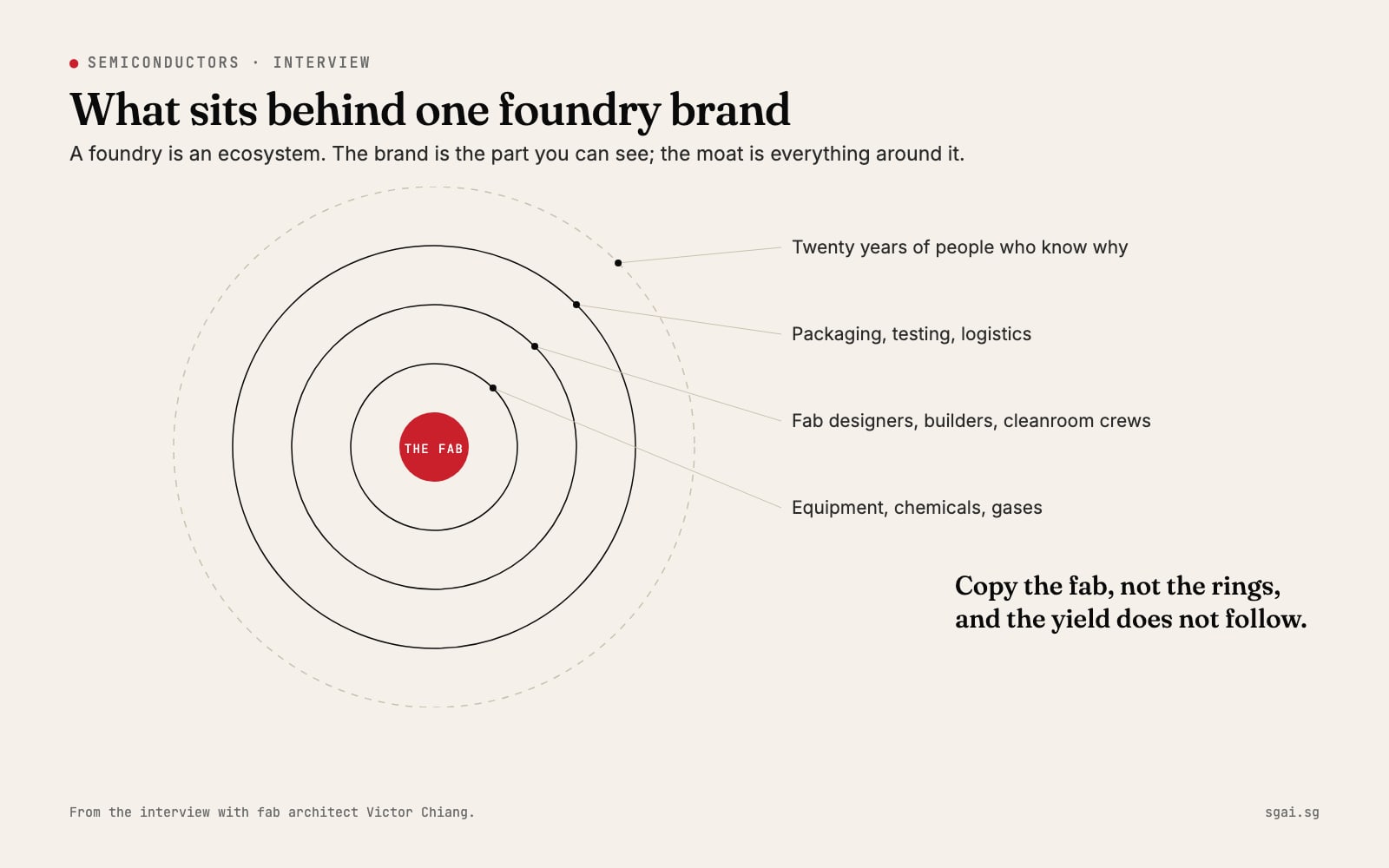
A senior architect who has spent two decades designing wafer fabs for Taiwan's leading foundries explains the supply chain ecosystem behind Taiwan's grip on advanced chip manufacturing — including the lunchbox-maker that became a critical-path supplier, the IPO'd cleaning specialists, the heavy crane firm built specifically to lift ASML EUV machines, and the Sunday-night phone call that built Nvidia.
Most coverage of Taiwan's semiconductor industry stops at the foundry brand on the headlines. We sat down with Victor Chiang, a senior architect and engineering consultant who has spent 20+ years designing wafer fabs for Taiwan's leading foundry clients — from his first project in 2000 to today — to talk about what actually makes the moat. The answer turns out to be neither lithography nor process recipes alone. It's an ecosystem of dozens of specialist suppliers, many of them obscure, that the foundry pulled up around itself over three decades.
The names of Victor's foundry clients have been masked at his request. Where he refers to "the major foundry," he's describing a top-tier Taiwan-headquartered semiconductor manufacturer. The technical details, anecdotes, and timelines are all as he related them.
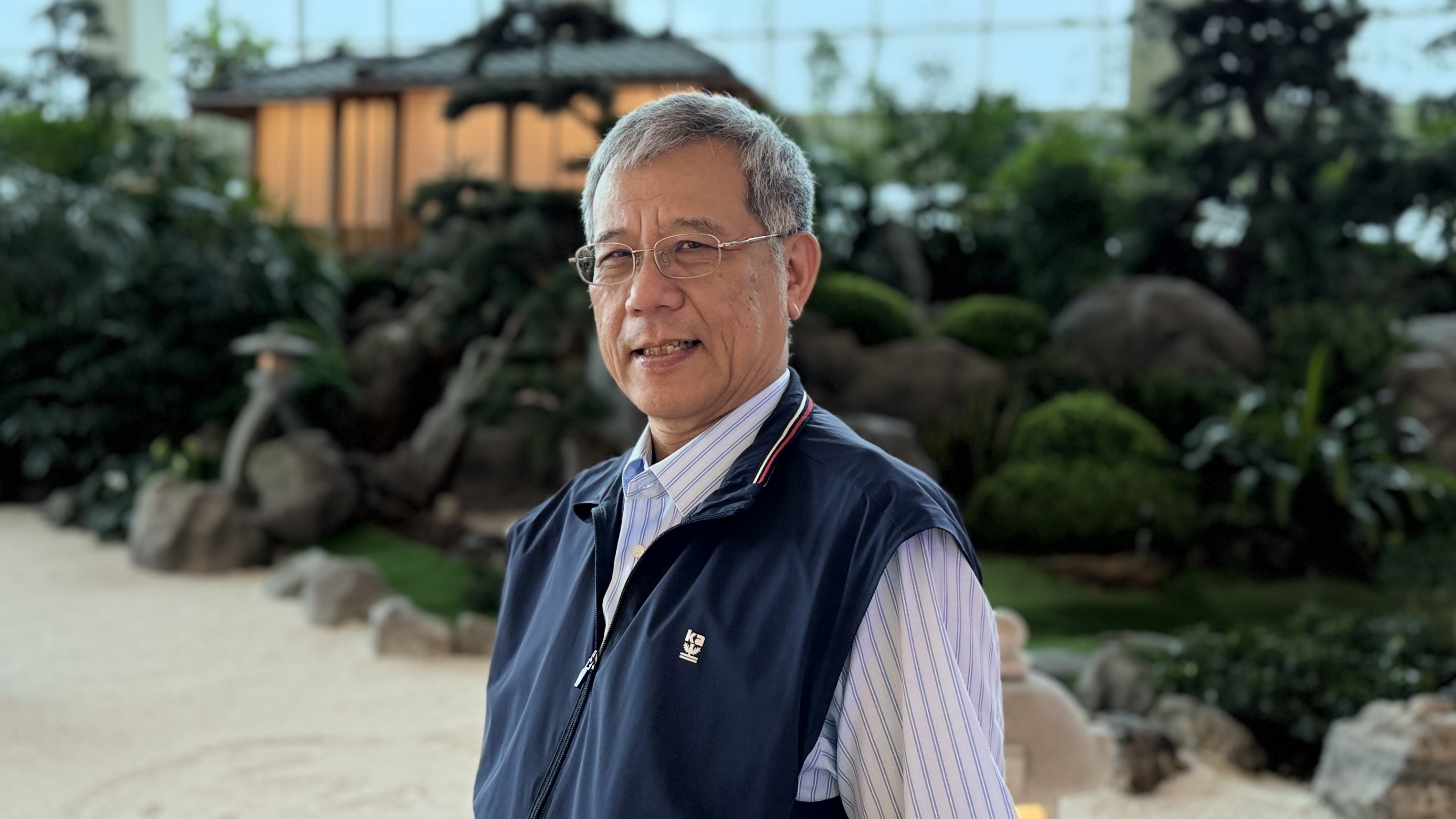
Victor Chiang — semiconductor architect, 20+ years of wafer-fab design across Asia. Photographed by SGAI Studio.
Why Victor's perspective matters
Most people who could tell this story can't. Foundry employees are bound by NDAs that keep them off the record entirely. Chip designers see one slice of the picture and have a product roadmap to defend. Equipment vendors are selling something. Government officials and analysts have a brand to protect or a thesis to push.
Victor sits in the rarest seat in the entire industry: the architect. He designs the physical buildings inside which the chips are made — which means he sees the whole ecosystem (design, build-out, equipment install, ramp, operations, supplier coordination, regulatory interaction) from close range, but he doesn't sell chips, doesn't write the process recipes, and doesn't take public positions on geopolitical questions. He's the closest thing to a credible bystander the semiconductor industry has — close enough to know how it really works, independent enough to talk about it on the record.
For Singapore readers, this matters in a particular way. Singapore's AI strategy is built on top of a 60-year semiconductor manufacturing base. The people who understand that base most clearly are not the ones in the headlines — they're the ones who have spent decades building the physical infrastructure that makes the headlines possible. Victor is one of them.
A 60-second primer for non-technical readers
What is a semiconductor? A thin slice of silicon, etched with billions of microscopic transistors, that acts as the brain of every modern electronic device — from your phone to a heart-rate monitor to an AI server.
Why semiconductor = AI. Every AI model — ChatGPT, Claude, hospital diagnostic tools, factory inspection systems — runs on chips. The most advanced AI training runs on the most advanced chips. AI embedded inside physical products (medical devices, industrial sensors, vehicles, robots) runs on a wider range of chips. Without semiconductor manufacturing, there is no AI economy.
Why Singapore cares. Singapore has been building semiconductor manufacturing capacity for nearly 60 years — since Texas Instruments opened its first Singapore assembly plant in 1968. The country's current S$37 billion AI commitment under Budget 2026 is the latest chapter in a long arc, not a sudden new direction. The new VSMC fab in Tampines (Vanguard + NXP, US$7.8 billion) is part of the same arc. We've broken down the SME implications of that fab in a companion piece.
Q1. How did you get into fab design? What was the industry like when you started?
I started in semiconductor fab design around 2000–2001. Before that I'd had a more general architecture background — I'd actually spent five years in South America in the late 1980s, working with computers there for the first time, then came back to Taiwan in the early 1990s and joined an architecture firm in 1993.
When I first started touching this industry around 2000, the wafers were 4-inch and 6-inch — small. The process was thick — micron scale, not the nanometre scale of today. The chips back then ran hot, and the way I describe it to people is: the whole game in chips is heat. Once a chip gets hot, performance falls. So the entire industry has spent 25 years finding ways to make chips thinner and run cooler.
By 2006 I had a much fuller picture of how the supply chain actually worked, because we'd been building more fabs and our interaction with owners was much closer. Before then, honestly, I didn't really understand the ecosystem.
Q2. You told me earlier that "heat is the enemy" — and that there's a famous example involving Apple, Samsung, and the major foundry. What happened?
Apple at one point was sourcing the same CPU model from both the major foundry and Samsung. People online actually pulled both apart and benchmarked them.
The major foundry's part was 16nm. Samsung's was 14nm — supposed to be more advanced. But in practice the 16nm part ran more stably and dissipated heat better. It just didn't pile up heat the way Samsung's did.
After that incident, Samsung kept getting tripped up by the heat issue. Customers started looking specifically at which foundry made the chip before they'd buy it — and from then on, everyone designing CPUs went to the major foundry. That was years ago. Things have improved since. But the original incident was really wild.
This is what I mean by "heat is the moat." It's not just thinner is better — it's that thinner is only better if you can get it without piling up heat. Yield is downstream of that.
Q3. The Nvidia origin story — you said earlier this is widely known but most outsiders don't realise how much it shaped the industry. Tell me what happened.
When Nvidia first started out — they were doing compute chips, the kind of math accelerators that everyone's PC now needs — they couldn't find a foundry to fab their chips. They went to Intel. They went to one other (I forget the name). They even went to Samsung. Nobody would do it. Nvidia was a small company at the time and the big players didn't want the business.
Morris Chang, the major foundry's chairman, picked up the phone and said: "No problem. I'll fab your chips."
That's it. From then on, the major foundry has supported Nvidia all the way through. That's why Nvidia is so loyal to them today.
There's a Chinese cultural element to this — what we call "delivering charcoal in the snow." Western firms tend to be more transactional: if there's no commercial upside for me, why would I help you? The major foundry itself was once on the receiving end of that exact attitude — early on, a team of about a dozen engineers flew to Germany to visit some company. They got all the way to the office front door and the receptionist told them "no time for you," and the entire team had to fly home.
Now it's the Germans asking the major foundry to come over and build a fab.
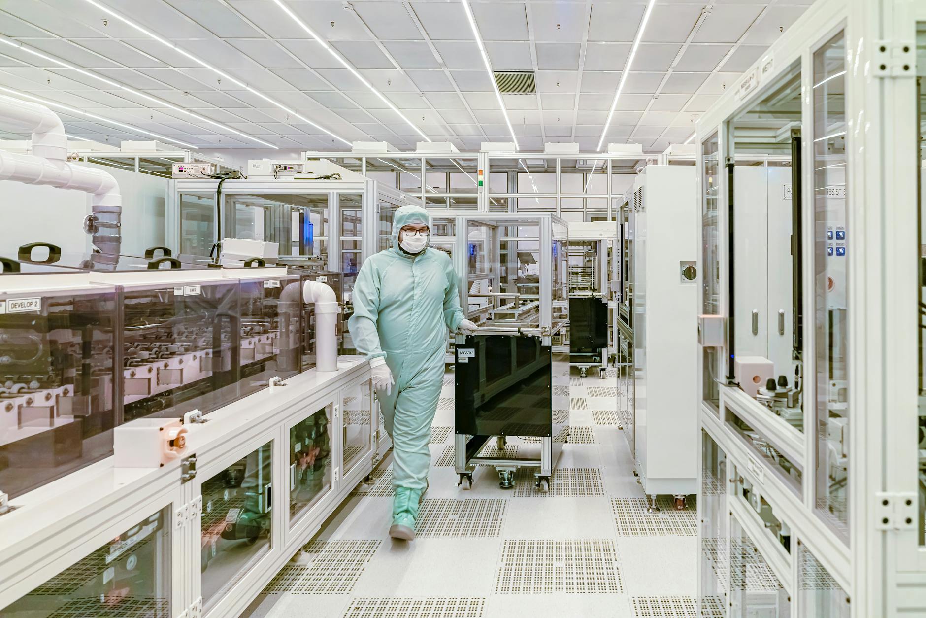
A modern semiconductor cleanroom — the kind of physical environment Victor Chiang designs the shell for. Photo: Российский центр гибкой электроники / Pexels.
Q4. The hidden supply chain — most people see one foundry brand and think of one company. You talk about it as an ecosystem. Walk me through some of the suppliers.
This is the part outsiders almost never see. People look at one foundry name and think the company. What they should see is the ecosystem that foundry pulled up around itself over decades. Most of the major foundry's critical-path suppliers were brought in, trained, and grown by the foundry itself.
A few examples I find interesting:
The vacuum carrier vendor. When you process a wafer you have to seal it inside a vacuum carrier — without it, dust gets in and the wafer is unusable. The vendor that makes those carriers used to make lunchboxes. The major foundry took them, helped them re-tool, and turned them into a critical supplier. They went from making bento containers to making the shells that hold the most expensive disks of silicon in the world.
The cleaning specialist. Cleaning fab equipment is its own technical discipline — it's not "wipe with a cloth." There's a company that does literally nothing else. They went IPO. Their entire business is keeping the major foundry's tools clean to spec.
The crane operator. Taiwan's biggest crane company, Qide (啟德), is one of the few in the world that can lift an ASML lithography machine — including EUV. Each EUV unit costs over US$200 million, and one bump means a write-off. The crane company built specialised rigs specifically to handle this work. Now every ASML machine — and the broader installed equipment — that comes into a major foundry fab gets lifted into position by them.
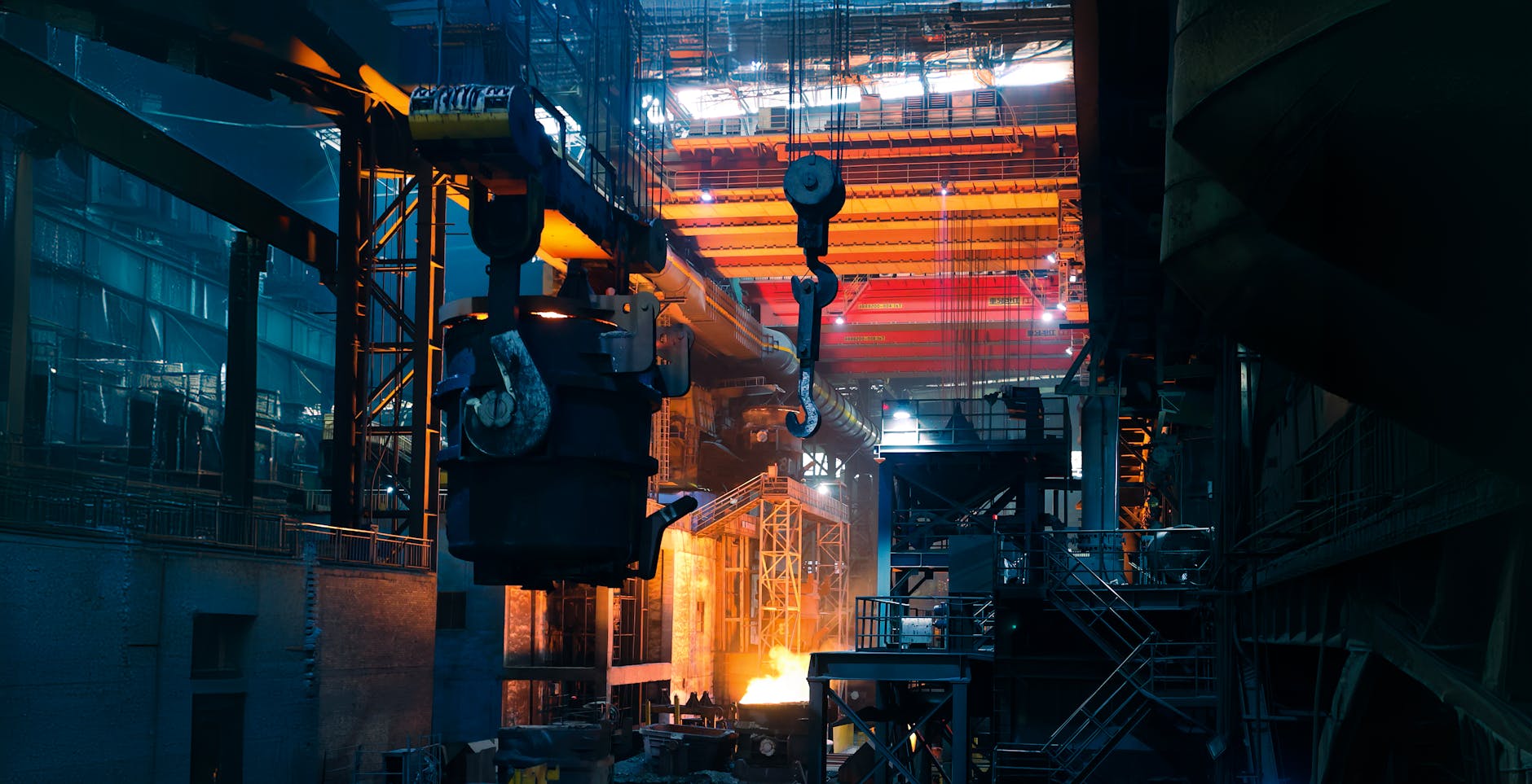
Heavy industrial cranes — Taiwan's Qide (啟德) built rigs specifically to lift US$200 million ASML EUV machines into the major foundry's fabs. Photo: jason hu / Pexels.
You can multiply this story across dozens of suppliers — quality control, calibration, packaging, materials handling. None of it is replicable with money or time alone. It takes decades of mutual investment between the foundry and each specialist.
This is why I think Jensen Huang at Nvidia has said publicly that Elon Musk is being too simple about this. Musk can't just spin up a fab elsewhere and replicate this. Jensen understands the major foundry's ecosystem better than most because he lives inside it.
Q5. You mentioned that even yield is partly an ecosystem effect, not just a process recipe. Can you explain?
Yield comes down to "how many process passes" you need. For the same 12-inch wafer, the major foundry might hit yield in around 200 process passes. Intel and Samsung might need 300, even 350 passes for the same generation.
More passes = higher cost. And the yield isn't even guaranteed to catch up. The major foundry's 200-pass capability is their know-how — they're not going to tell you exactly how they do it. But part of the answer is that every step in those 200 passes depends on supplier components and processes that were co-developed over decades.
If your supplier base is weak, you can't run a 200-pass process reliably. You're forced into 300 passes just to get yield. Then your cost rises. Then your margin disappears. This is why the moat is real — it's not just one trick.
Q6. How fast can the major foundry actually build a fab?
The benchmark they cite publicly is 20 months from breaking ground to mass production. At the absolute limit, 24 months. The math works out like this:
- 24 months total
- Minus 6 months of commissioning ("trial run") = 18 months
- Minus 6–8 months of utility installation (cleanroom, HVAC, mechanical, electrical, MEP panels) = 10–12 months
- The actual building — foundation, structure, envelope — has to be delivered in roughly 12 months flat
And those 12 months don't include design. Design has to be complete before ground breaks. The architects, the foundry, and the local permitting authority operate as one tight unit. We've worked with the high-tech park management here for decades — relationships are tight enough that we sometimes split a single permit into two pieces, so piling can start while the structural permit is still being processed.
This level of operational coordination is hard to convey. Most countries genuinely cannot execute at this tempo.
Q7. What does designing the building actually involve? The technical depth of a leading-edge fab is invisible to most people.
Our scope is the shell — the building. Inside the shell, the foundry tells us what they need: how much space, how much clear height (for some cleanrooms it's 9 metres), where the slab needs holes, where there can't be columns, what loads to design for. We deliver a building that meets those specs and complies with code (seismic, fire, etc.). They install the actual fab equipment themselves, with vendors from Germany, Spain, the Netherlands, Sweden — multiple countries, all working in parallel.
One detail I always come back to: dirty air is heavy. So our cleanroom floors are designed with holes in them. The dirty air falls and is sucked out from below. Clean air is pushed in from above. The cleanroom is in constant circulation — that's how you get the particulate counts down to where the equipment needs them.
For micro-vibration — the tools are extremely sensitive — the foundry takes our drawings, runs them through their own simulation software, and checks compliance against spec. Only they know the spec. We design to the brief, they verify.
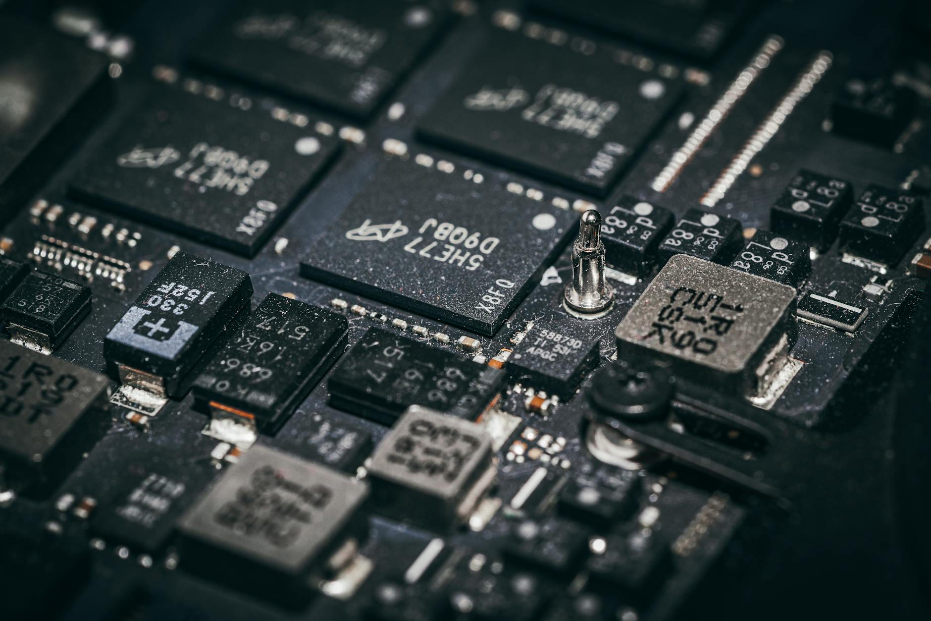
Silicon chips at macro detail — the end product of a 30-year ecosystem build-out, not a single company's process recipe. Photo: Jakub Pabis / Pexels.
Q8. You said something striking earlier — that AI is becoming hardware, not just software. What do you mean?
We're in a transitional phase. Most people today think of AI as ChatGPT — a website you type into. But the real long-term play is AI living inside physical objects: robots, vehicles, factory equipment, household devices, medical implants.
The clearest examples I see are in defense and space.
Space. Look at SpaceX. They land their rockets and put 20 satellites up in a single launch. The reason that works is AI — not the AI you talk to, the AI that lives inside the guidance computer doing the math in flight. NASA's Apollo 13 nearly didn't make it back because the trajectory math was being done by humans. Today's Artemis missions can loop the dark side of the moon and re-acquire signal at a precise predicted second because AI is doing the computation. No human can keep up with that.
Defense. Taiwan can now photograph PLA stealth aircraft — including J-20 — without ever scrambling its own jets. The detection equipment was supplied by the US and uses AI under the hood. The implication: I can't see you, but I can hit you. You can't see me. That's AI as hardware.
The medical version of this is going to be a chip in a pill or implanted directly. The industrial version is AI-controlled robotic manufacturing. The consumer version is your house knowing you're sick before you do.
None of it works without leading-edge chips, manufactured at scale, with reliable supply. That's why semiconductor capacity matters strategically — not just for AI servers, but for the whole next generation of physical-world AI applications.
Q9. One personal example — you said AI just helped you remember a technical term. What happened?
Last weekend an old colleague (from a contractor I used to work with) suddenly asked me a technical question. I needed to recall the name of the metal fastener used to hang the Geting wood panels in our local style of construction. I drew a blank. I asked an AI tool — instantly came back with the exact technical term: L-shaped metal bracket.
It's a small example but it's the right kind of example. That kind of speed-to-the-right-jargon was simply not possible before. And as I keep using these tools, the overlap between my way of thinking and the AI's responses keeps getting tighter. The trend is clear. AI's learning cycle is faster than any human's.
Q10. What's the one thing you'd want readers to take away?
That the foundry industry isn't a single company doing magic in a back room. It's a whole ecosystem that took 30 years to build, and the part most people see — the foundry name on the headlines — is the smallest visible part of it.
When people ask me whether [insert country] can replicate Taiwan's semiconductor industry, my answer is: with enough money and time, you can build a fab. With another decade of patient ecosystem investment, you might build the suppliers the fab needs. But the cultural attitude — delivering charcoal in the snow, the willingness to take on a small no-name customer because you believe in them — that's the part you can't buy. That's also why a single phone call from Morris Chang in the 1990s built what is now a multi-trillion-dollar relationship.
That's the part of the story I want more people to understand.
About Victor Chiang
Victor Chiang is a veteran semiconductor architect with 20 years of experience designing and overseeing semiconductor architecture for some of the most recognisable semiconductor manufacturers in the world. His work spans multiple high-tech park projects across Asia.
Victor's vantage point is what makes his perspective unusually valuable. He's not a foundry employee, so he's not bound by the NDAs that keep most semiconductor insiders from speaking publicly. He's not a chip designer, so he's not selling a product roadmap. He's the architect — the professional who designs the physical buildings inside which the chips get made — which means he sees the ecosystem from a position close enough to know how it actually works, but independent enough to talk about it on the record.
The names of his foundry clients are not disclosed in this interview at his request, in line with standard NDAs across the industry.
About SG AI Studio
SGAI Studio is a Singapore studio that connects AI with great businesses: AI digital modernisation for established companies, so they are found, understood and recommended by people and by AI assistants. We publish interviews like this one because the people who build the hardware rarely get asked how it actually works.